Material Characterization
Microscopy, SEM with EDS, XRD and related techniques that reveal a material’s structure and composition.
High-magnification imaging of surfaces with elemental analysis of selected areas.
A scanning electron microscope (SEM) uses a focused beam of electrons to image a sample’s surface structure and morphology at far higher magnification than an optical microscope. Energy-dispersive X-ray spectroscopy (EDS) uses the X-rays produced by the same beam to identify the elements present.
Features that decide how a material performs are often too small for an optical microscope. SEM shows them, and EDS identifies what they are made of, within the limits of the instrument and the sample.
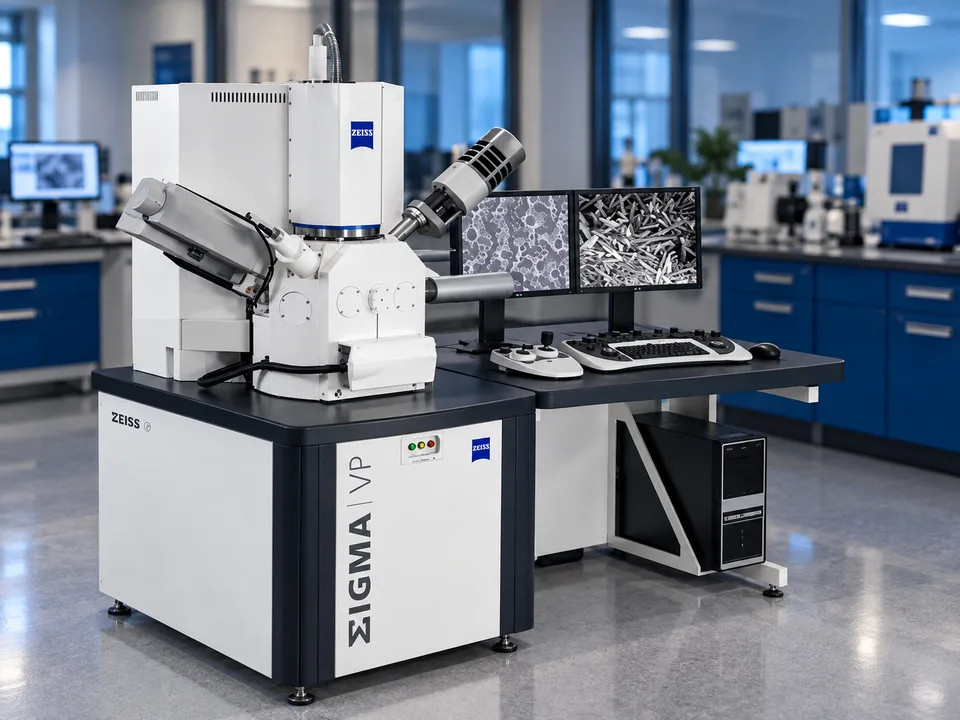
SEM analysis is carried out on a Zeiss Sigma field-emission instrument. See the instrument page for its specifications.
Samples must be solid, dry and able to fit the chamber. Non-conductive samples may need a conductive coating. Tell us about your material and we will advise.
No. EDS identifies and estimates the elements in a small area near the surface. It is well suited to comparing regions and identifying particles or inclusions, but it is not a substitute for bulk chemical analysis.
Timing depends on the number of samples and instrument scheduling. We will give you an estimate when you enquire.
Microscopy, SEM with EDS, XRD and related techniques that reveal a material’s structure and composition.
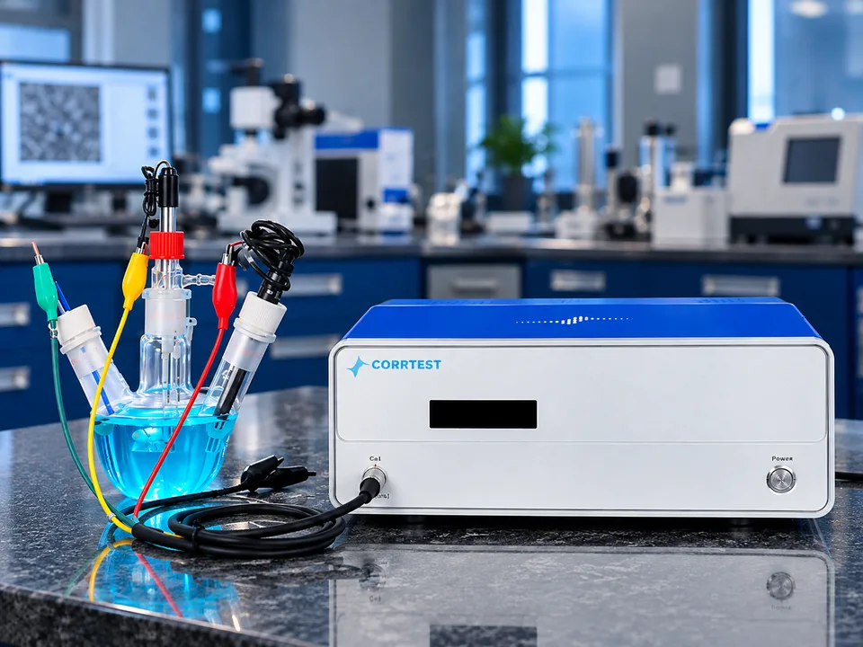
Contact angle, surface roughness, wear and corrosion tests that describe how a surface performs in service.
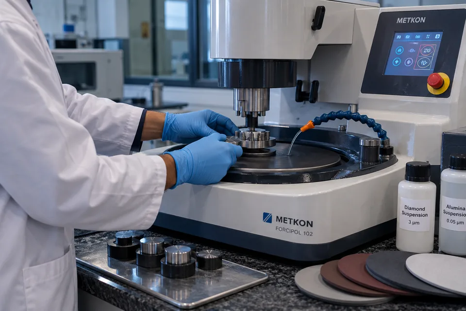
Cutting, mounting, grinding, polishing and etching to prepare specimens for testing and microscopy.
Tell us about your sample and testing objective, and our team will help you decide the appropriate next step.